It can be an amplifier or a switch, but today let’s put down notes about switches because I found them more interesting:
Silicon is a semiconductor
- 4 valence electrons
- Tetrahedral crystal
Doping a semiconductor n-type doping:
- injecting a small amount of an element like Phosphorus, which is similar to silicon and has 5 valence electrons. Having one more than silicon makes the conductivity better
- it’s the negative electrons that move p-type
- an element with 3 valence electrons like Boron. That way it creates a hole that also increases the conductivity, because the electrons can move into the hole itself
- the hole, which is a lack of an electron, actually acts like a positive charge, and that’s why it’s the “P” type. The movement here is of the holes themselves By the way, that doesn’t mean they are actually positive and negative, but neutral, because of the number of electrons and protons inside
Transistor are made of P-Type and N-Type doping
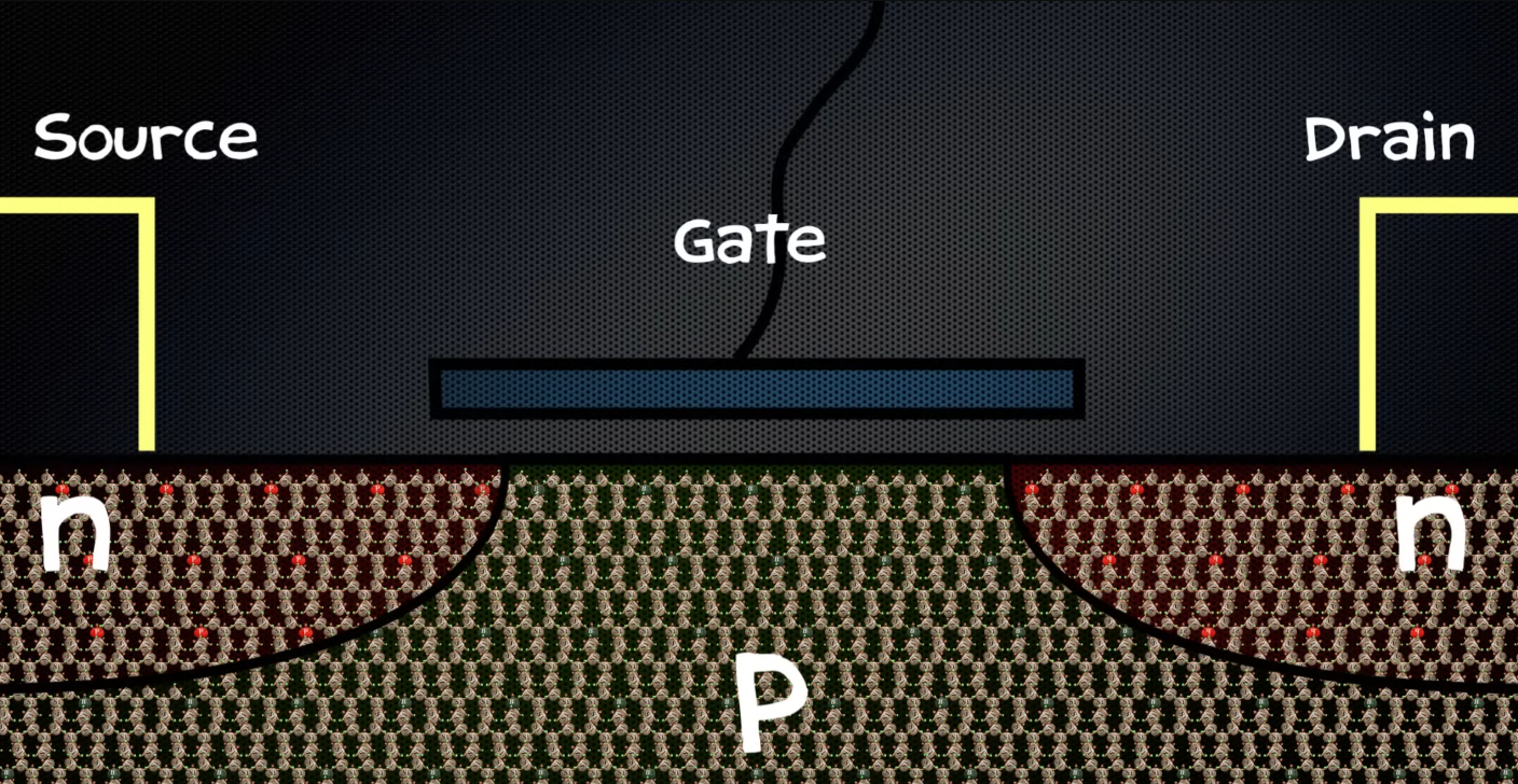
Figure 1 - Transistor built from P-type and N-type doping
There are electrical contacts at the ends/edges, and there is an electrical contact in the middle isolated by an oxide layer (the gate)
In the area between P and N, the N-type electrons move to the P-type and create something called a depletion area. There are no free electrons in the n-type because they filled the P’s holes
- This makes the P-type repel electrons that try to come across from the N-type, acting like a barrier This depleted area prevents the electrons from flowing through the transistor, so the transistor’s state is off. It’s like an open switch (the zero state)
To turn it on, it needs a small positive voltage applied to the gate, attracting the electrons through the gate and making them form a conducting channel
- It makes the transistor on, in the one state Continuation in logic gates